|
Electronics |
||
|
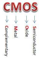
CMOS
CMOS would be the most important component (I would call it a concept rather than a component) in modern electronics. It stands for Complimentary Metal Oxide Semiconductor. The term MOS here refer to MOSFET.
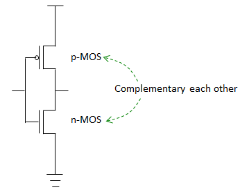
Now you would have a lot of questions (You must have.. if you are new to this area). What does it mean by 'Complementary' ? What is Metal ? What is Oxide ? What is MOS ? etc. Regarding MOS/MOSFET, I would post separate pages since it would be pretty long story by itself. Just a little bit comments on the word. When some things (usually two things) operating in a kind of oposite manner work together to achieve a single/unified function, we call it 'complementary'. In the context, 'Complementary' means two different types of MOSFET (p-MOS and n-MOS) operating in opposite manner working togather to achieve a combined functionality. The most common/simple CMOS you would have seen in all the textbook and reading material is as follows. This is not the only possible configuration of CMOS circuit, but in any kind of CMOS circuit you will see both p-MOS and n-MOS get involved and working together to achieve the overall function of the circuit.
Follwoings are the list of topics that will be covered in this page.
Why we use CMOS so widely these days ? What are the advantages of CMOS comparing to other logics (e.g, TTL). Followings are some of the items that are commonly mentioned as the merits of CMOS.
Now let's look at several examples of practical application of this CMOS concept.
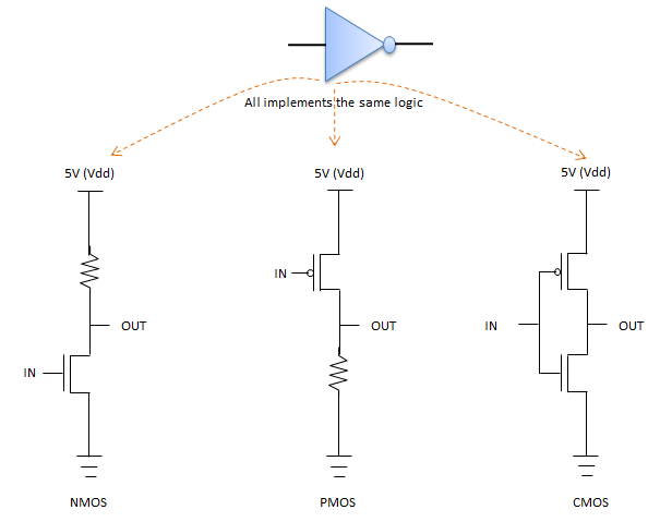
The simplest application of CMOS would be to implment 'NOT' Gate. (I assume that everybody knows what NOT gate do. Simply put, if it takes in '1', it puts out '0' and if it takes in '0', it puts out '1'). There can be many ways to implement this logic, but you can think of roughly 3 different ways to implement it if you want to use MOSFET as shown below. (To understand the details on how these circuit can implement the 'NOT' logic, you need to have basic understanding of Transister, MOSFET, Pull-Down/Pull-Up Resitor and knows how to calculate the voltage at a specific point in a circuit made up of bunch of resistors. For now, I assume that you've already have all these basic understanding.)
Since this is the page for CMOS, I will explain only about the implementation using CMOS.
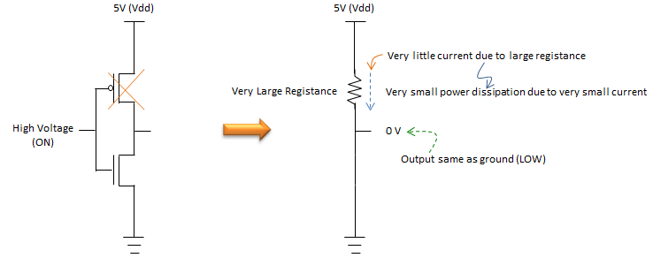
First, let's think about the case where '1' is coming into the input port, meaning the high level voltage is applied to the input pin. Then the operation of each MOS is as shown on left in the following illustration. The cross mark (X) indicate that the specific MOS is turned off. It means the current through the turned-off transister is very small (negligible). The very small current means very large resistance. The MOS without the cross mark means it is turned on. It means current can go through the MOS as much as it is allowed, meaning there is almost no resistance. If you apply this logic, you can convert the CMOS circuit into a simple resistor circuit as shown on right. Once you get this kind of resistor circuit, you would be able to figure out the voltage being applied to the output port. In this case, 0 V will be measured at the output port indicating the logic '0'
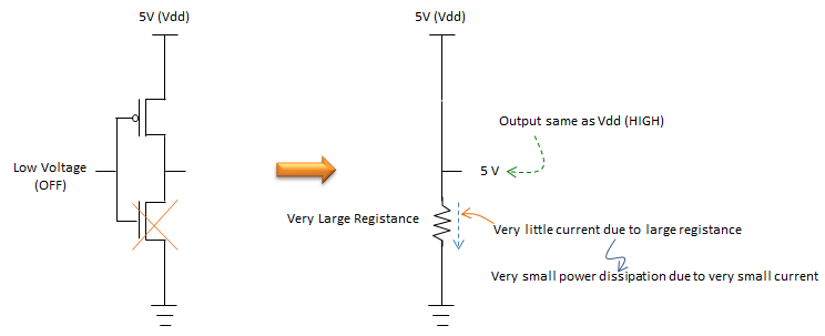
Now, let's think about the case where '0' is coming into the input port, meaning the low level voltage is applied to the input pin. Then the operation of each MOS is as shown on left in the following illustration. The cross mark (X) indicate that the specific MOS is turned off. It means the current through the turned-off transister is very small (negligible). The very small current means very large resistance. The MOS without the cross mark means it is turned on. It means current can go through the MOS as much as it is allowed, meaning there is almost no resistance. If you apply this logic, you can convert the CMOS circuit into a simple resistor circuit as shown on right. Once you get this kind of resistor circuit, you would be able to figure out the voltage being applied to the output port. In this case, 5 V will be measured at the output port indicating the logic '1'
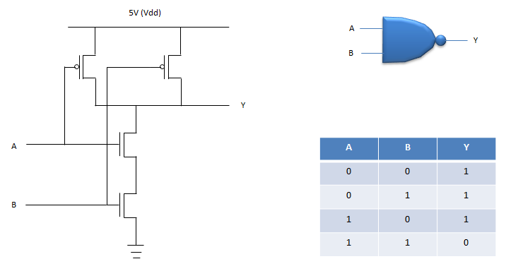
Now let's look into a little bit more complicated circuit. In this section, we will look into how we can implement NAND Gate using CMOS circuit. The CMOS circuit is show on left. You see the structure of the circuit is different from what we saw in previous section, but still we see two different types of MOSFET (p-MOS and n-MOS) working together (complementing each other) to achieve a common function (NAND function in this case). so this is also a kind of CMOS. The truth table for this circuit and the NAND gate symbol is shown on right.
Now let's look at how this CMOS circuit can implement NAND logic.
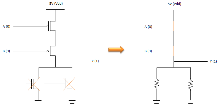
First, let's think about the case where '0' is coming into the both input A and B, meaning the low level voltage is applied to the both input pins. Then the operation of each MOS is as shown on left in the following illustration. The cross mark (X) indicate that the specific MOS is turned off. It means the current through the turned-off transister is very small (negligible). The very small current means very large resistance. The MOS without the cross mark means it is turned on. It means current can go through the MOS as much as it is allowed, meaning there is almost no resistance. If you apply this logic, you can convert the CMOS circuit into a simple resistor circuit as shown on right. Once you get this kind of resistor circuit, you would be able to figure out the voltage being applied to the output port. In this case, 5 V will be measured at the output port indicating the logic '1'
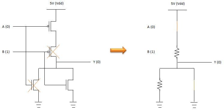
Now, let's think about the case where '0' is coming into the input A and '1' is coming into the input B, meaning the low level voltage is applied to the input 'A' pin and the high level voltage is applied to the input 'B' pin. Then the operation of each MOS is as shown on left in the following illustration. The cross mark (X) indicate that the specific MOS is turned off. It means the current through the turned-off transister is very small (negligible). The very small current means very large resistance. The MOS without the cross mark means it is turned on. It means current can go through the MOS as much as it is allowed, meaning there is almost no resistance. If you apply this logic, you can convert the CMOS circuit into a simple resistor circuit as shown on right. Once you get this kind of resistor circuit, you would be able to figure out the voltage being applied to the output port. In this case, 5 V will be measured at the output port indicating the logic '1'
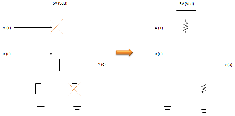
Now, let's think about the case where '1' is coming into the input A and '0' is coming into the input B, meaning the low high voltage is applied to the input 'A' pin and the low level voltage is applied to the input 'B' pin. Then the operation of each MOS is as shown on left in the following illustration. The cross mark (X) indicate that the specific MOS is turned off. It means the current through the turned-off transister is very small (negligible). The very small current means very large resistance. The MOS without the cross mark means it is turned on. It means current can go through the MOS as much as it is allowed, meaning there is almost no resistance. If you apply this logic, you can convert the CMOS circuit into a simple resistor circuit as shown on right. Once you get this kind of resistor circuit, you would be able to figure out the voltage being applied to the output port. In this case, 5 V will be measured at the output port indicating the logic '1'
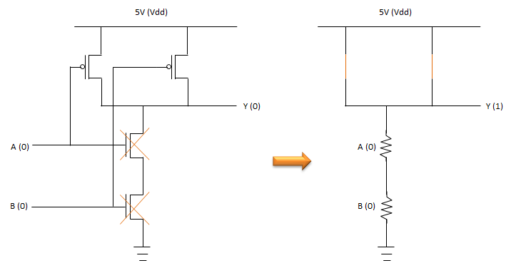
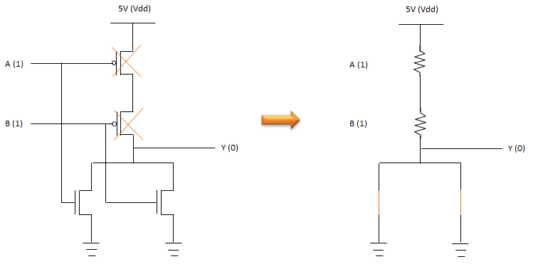
Lastly, let's think about the case where '1' is coming into the both input A and B, meaning the high voltage is applied to both input 'A' pin and 'B' pin. Then the operation of each MOS is as shown on left in the following illustration. The cross mark (X) indicate that the specific MOS is turned off. It means the current through the turned-off transister is very small (negligible). The very small current means very large resistance. The MOS without the cross mark means it is turned on. It means current can go through the MOS as much as it is allowed, meaning there is almost no resistance. If you apply this logic, you can convert the CMOS circuit into a simple resistor circuit as shown on right. Once you get this kind of resistor circuit, you would be able to figure out the voltage being applied to the output port. In this case, 0 V will be measured at the output port indicating the logic '0'
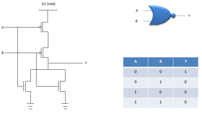
Now let's look into another common CMOS circuit as the one explained in previous section. In this section, we will look into how we can implement NOR Gate using CMOS circuit. The CMOS circuit is show on left. You see the structure of the circuit is different from what we saw in previous section, but still we see two different types of MOSFET (p-MOS and n-MOS) working together (complementing each other) to achieve a common function (NAND function in this case). so this is also a kind of CMOS. The truth table for this circuit and the NAND gate symbol is shown on right.
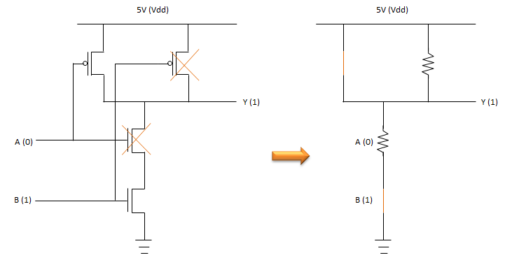
First, let's think about the case where '0' is coming into the both input A and B, meaning the low level voltage is applied to the both input pins. Then the operation of each MOS is as shown on left in the following illustration. The cross mark (X) indicate that the specific MOS is turned off. It means the current through the turned-off transister is very small (negligible). The very small current means very large resistance. The MOS without the cross mark means it is turned on. It means current can go through the MOS as much as it is allowed, meaning there is almost no resistance. If you apply this logic, you can convert the CMOS circuit into a simple resistor circuit as shown on right. Once you get this kind of resistor circuit, you would be able to figure out the voltage being applied to the output port. In this case, 5 V will be measured at the output port indicating the logic '1'
Now, let's think about the case where '0' is coming into the input A and '1' is coming into the input B, meaning the low level voltage is applied to the input 'A' pin and the high level voltage is applied to the input 'B' pin. Then the operation of each MOS is as shown on left in the following illustration. The cross mark (X) indicate that the specific MOS is turned off. It means the current through the turned-off transister is very small (negligible). The very small current means very large resistance. The MOS without the cross mark means it is turned on. It means current can go through the MOS as much as it is allowed, meaning there is almost no resistance. If you apply this logic, you can convert the CMOS circuit into a simple resistor circuit as shown on right. Once you get this kind of resistor circuit, you would be able to figure out the voltage being applied to the output port. In this case, 0 V will be measured at the output port indicating the logic '0'
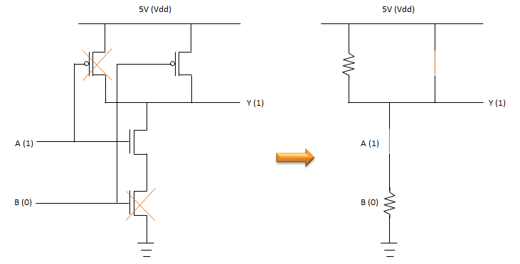
Now, let's think about the case where '1' is coming into the input A and '0' is coming into the input B, meaning the low high voltage is applied to the input 'A' pin and the low level voltage is applied to the input 'B' pin. Then the operation of each MOS is as shown on left in the following illustration. The cross mark (X) indicate that the specific MOS is turned off. It means the current through the turned-off transister is very small (negligible). The very small current means very large resistance. The MOS without the cross mark means it is turned on. It means current can go through the MOS as much as it is allowed, meaning there is almost no resistance. If you apply this logic, you can convert the CMOS circuit into a simple resistor circuit as shown on right. Once you get this kind of resistor circuit, you would be able to figure out the voltage being applied to the output port. In this case, 0 V will be measured at the output port indicating the logic '0'
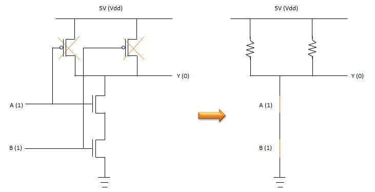
Lastly, let's think about the case where '1' is coming into the both input A and B, meaning the high voltage is applied to both input 'A' pin and 'B' pin. Then the operation of each MOS is as shown on left in the following illustration. The cross mark (X) indicate that the specific MOS is turned off. It means the current through the turned-off transister is very small (negligible). The very small current means very large resistance. The MOS without the cross mark means it is turned on. It means current can go through the MOS as much as it is allowed, meaning there is almost no resistance. If you apply this logic, you can convert the CMOS circuit into a simple resistor circuit as shown on right. Once you get this kind of resistor circuit, you would be able to figure out the voltage being applied to the output port. In this case, 0 V will be measured at the output port indicating the logic '0'
Reference :
[1] HOW CMOS WORKS: MOSFETS, JFETS, IGFETS AND MORE
|
||